Get ready for a groundbreaking development in 3D printing! Researchers have just unveiled an easy-to-build, low-cost 3D nanoprinting system that can create incredibly detailed structures. This cutting-edge technique is so precise that it can print metamaterials, microlenses, and other optical devices. The possibilities are endless!
According to Cuifang Kuang, the leader of the research team from Zhejiang Lab and Zhejiang University in China, “Our system uses a two-step absorption process to realize 3D printing with accuracy reaching the nanometer level, which is suitable for commercial manufacturing. It can be used for a variety of applications such as printing micro or nanostructures for studying biological cells or fabricating the specialized optical waveguides used for virtual and augmented reality devices.”
What sets this new system apart is its affordability and ease of use. Unlike conventional high-resolution 3D nanoprinting approaches that require expensive lasers, this system utilizes an integrated fiber-coupled continuous-wave laser diode that is both inexpensive and user-friendly.
“This new approach helps make 3D nanoprinting accessible to scientists, even ones who are not familiar with the optical systems typically used for this type of fabrication,” said Kuang. “It could eventually lead to low-cost desktop 3D nanoprinting devices that could offer precision nanoprinting to anyone.”
Creating a simple setup
When it comes to 3D printing objects with a feature size of approximately 100 nm, a technique called two-photon absorption is usually required. However, the researchers have developed a simplified and faster alternative called two-step absorption. This new approach uses a special photoinitiator and a single light source to achieve polymerization. The system utilizes a 405-nm-wavelength integrated fiber-coupled laser, making it more efficient and cost-effective.
The laser beam is directed onto galvanometric mirrors and then focused into the photosensitive material using a high-numerical aperture microscope objective. This streamlined process eliminates the need for numerous optical components, saving money and reducing errors.
Printing tiny objects
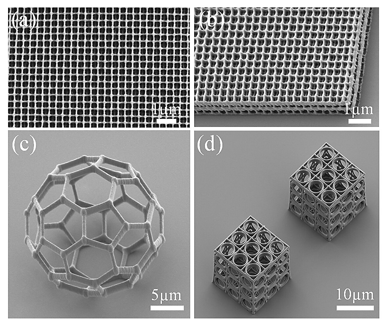
The researchers have successfully demonstrated the capabilities of their 3D nanoprinting system by printing 2D line gratings and 3D woodpile nanostructures. Even at low speeds, the system can achieve impressive resolutions and linewidths. The team is now focused on improving the writing speed and quality of the technique while maintaining high resolution, making it even more versatile for various applications.