Directing light from place to place is the backbone of our modern world. Beneath the oceans and across continents, fiber optic cables carry light that encodes everything from YouTube videos to banking transmissions—all inside strands about the size of a hair.
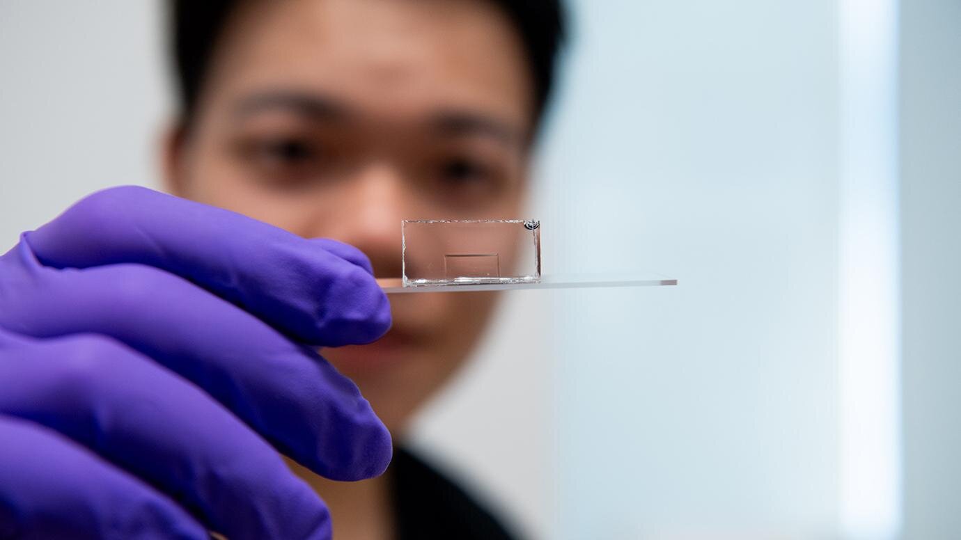
But what if we could make these strands even thinner and flatter, so thin that they’re actually 2D instead of 3D? University of Chicago Prof. Jiwoong Park and his team wondered about this possibility and conducted innovative experiments to find out.
They discovered that a sheet of glass crystal just a few atoms thick could trap and carry light. Not only that, but it was surprisingly efficient and could travel relatively long distances—up to a centimeter, which is very far in the world of light-based computing.
Their research, published in Science, showcases the development of 2D photonic circuits and the potential for new technology.
“We were utterly surprised by how powerful this super-thin crystal is; not only can it hold energy, but deliver it a thousand times further than anyone has seen in similar systems,” said lead study author Jiwoong Park.
Guiding light
The newly invented system is a way to guide light—known as a waveguide—that is essentially two-dimensional. The researchers found they could use extremely tiny prisms, lenses, and switches to guide the path of the light along a chip—all the ingredients for circuits and computations.
Unlike existing waveguides, where photons always travel enclosed inside, this system allows part of the photon to stick out of the crystal as it travels. It’s like setting suitcases on top of a conveyer belt instead of enclosing them in a tube. This approach makes it much easier to build intricate devices with the glass crystals, as the light can be easily moved with lenses or prisms.
Furthermore, the photons can gather information about the conditions along the way, making it possible to create microscopic sensors. For example, these waveguides could be used to sense the presence of specific molecules in a liquid sample.
The scientists are also interested in building very thin photonic circuits that can be stacked to integrate more tiny devices into the same chip area. While the experiments used molybdenum disulfide, the principles should work for other materials.
Realizing this behavior in the laboratory was a challenging but satisfying journey for the scientists. “Everything we needed we had to devise ourselves—from growing the material to measuring how the light was moving,” said graduate student Hanyu Hong, co-first author of the paper.